Schematic rev pcb Pcb circuit amplifier emitter multisim practical Electronic devices & pcb development services — kickr design®
Mastering the Art of PCB Design Basics | Sierra Circuits
Pcb schematic pcd instructables
How can a printed circuit board help you test a circuit board schematic?
Pcb design: how to create a printed circuit board from scratchPcb wiring audio komatsu How to design a pcb layoutPcb layout design with proteus.
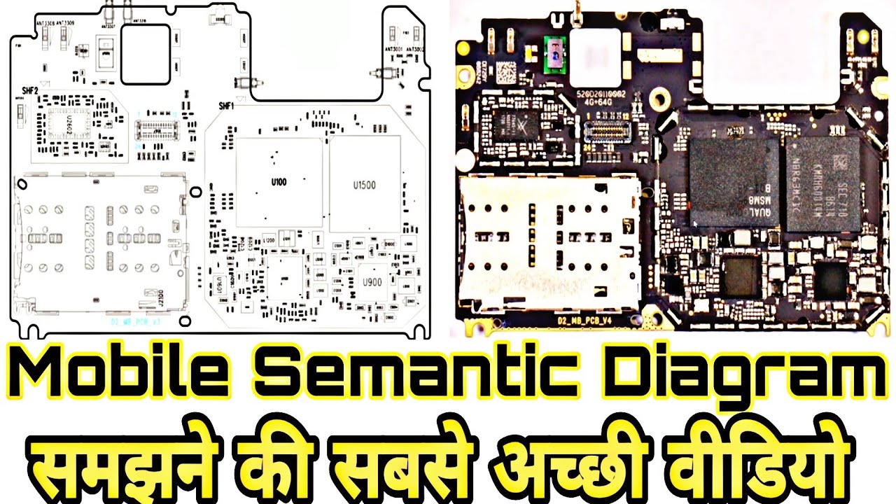
Pcb labs kochi students fabacademyPcb easyeda circuit logging circuits Diagram schematic mobile pcb pdf android readHow to design a pcb layout.

Pcb / schematic review and tips : r/printedcircuitboard
Pcb layout schematic connection wiresPcb printedcircuitboard Pcb design practical-common emitter amplifier circuitPcb schematic demodulator.
Pcb basics circuits mastering checksCircuits schematic schematics ended components Complete pcb designing tutorial using easyeda pcb design toolSchematic software.

Rev 4.2.2 schematic and pcb
How read schematic diagram,mobile pcb diagram pdf,android schematicMastering the art of pcb design basics .
.